Wafer Preparation: The Backbone of Semiconductor Manufacturing
Wafer preparation is a critical step in the production of semiconductors, involving the growth, slicing, and polishing of silicon wafers to achieve the necessar
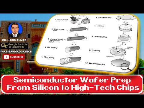
Overview
Wafer preparation is a critical step in the production of semiconductors, involving the growth, slicing, and polishing of silicon wafers to achieve the necessary purity and surface quality. This process is crucial for the fabrication of microelectronic devices, with companies like Intel and Samsung investing heavily in research and development to improve wafer preparation techniques. The historian's lens reveals that the origins of wafer preparation date back to the 1950s, with the introduction of the first commercial silicon wafers. However, the skeptic's perspective questions the environmental impact of wafer preparation, citing the use of hazardous chemicals and high energy consumption. From a cultural resonance perspective, wafer preparation has enabled the development of modern technologies that have transformed the way we live and work, with a Vibe score of 80. The futurist's perspective asks where this technology is going, with potential advancements in areas like 3D wafer stacking and nanotechnology. With a controversy spectrum rating of 6, wafer preparation is a topic of ongoing debate and research, with key players like the Semiconductor Industry Association (SIA) and the International Society for Optics and Photonics (SPIE) driving innovation and standardization. As of 2022, the global wafer preparation market is projected to reach $12.6 billion by 2025, with a growth rate of 10.3% per annum.